 Tweet
Tweet
I just wanted to share my experience and suggestions for fixing MB that may appear to be dead due to BIOS flashing failure or after an incorrect BIOS was flashed. I hope this procedure will help other people who thought their MB was bricked. I'm pretty sure that similar procedure can be used for most dual BIOS motherboards.
<hr>Assumptions:
My problem with EP45-UD3P occured after I flashed the F9 BIOS. The flashing process appeared to finish fine however it did stuck in the middle for a few seconds while writing one of the blocks (I wonder if that was the root cause of the problem). After reboot the system would never detect any RAM, no matter what I did. I tried everything suggested in these forums and elsewhere but nothing worked.
The MB supposes to detect defective main BIOS and fall back to the previous version of the BIOS preserved in the second backup chip. However for some reason my MB would not do it.
Microelectronics is one of my hobbies so finally I decided to look for the spec of the BIOS chip in order to try disabling the main BIOS chip temporarily so it would become "invisible" and allow the backup BIOS to be loaded.
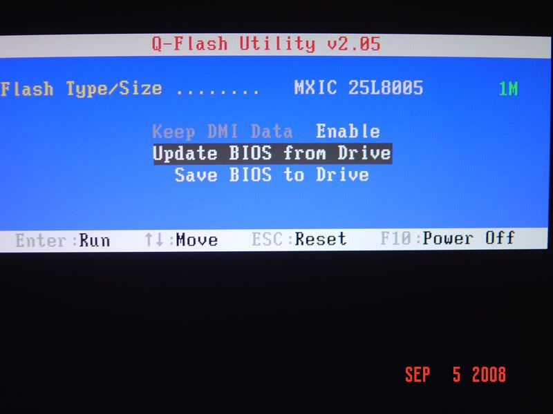
EP45-UD3P uses two identical MX25L8005 serial flash memory chips: one for each BIOS. Here is the datasheet.
According to the datasheet it is possible to prohibit reading from and writing to the chip by connecting pins 4 (GND) and 7 (#HOLD). The trick I was going to play was to disable the main chip and re-enabling it as soon as the backup BIOS loaded.
The chips are rather small and connecting wrong pins may damage the MB. I soldered a small button between pins 4 and 7 of the main BIOS chip so that I could connect and disconnect them easily. The distance between the pins is about 8 millimeters. If you have steady hands then you can use micro tweezers or similar tool instead.
Here is the picture of the right lower corner of the EP45-UD3P that shows location of both BIOSes (M_BIOS is the main one and B_BIOS is the backup).

Each BIOS chip has 8 pins. Pin 1 is marked with blue dot in the left lower corner of each chip. The pins are numbered in circle going counterclockwise. The red line shows connection between pins 4 (the rightmost at the bottom) and 7 (the second left at the top) of the main BIOS chip.
Once the button has been soldered the procedure is very simple:
IMPORTANT:
Always disconnect power before soldering, use grounding and protect you system from static electricity.
<hr>Assumptions:
- This is a dual BIOS MB (mine was Gigabyte EP45-UD3P v1.1).
- You have good eyes and steady hands (good soldering skills may help but aren't necessary).
- Your second (backup) BIOS is still correct (this is usually the case).
- You have miniature tweezers that can be used to connect two small pins (any other suitable tool will do).
- You agree not to hold me responsible for any damage and/or loss.
My problem with EP45-UD3P occured after I flashed the F9 BIOS. The flashing process appeared to finish fine however it did stuck in the middle for a few seconds while writing one of the blocks (I wonder if that was the root cause of the problem). After reboot the system would never detect any RAM, no matter what I did. I tried everything suggested in these forums and elsewhere but nothing worked.
The MB supposes to detect defective main BIOS and fall back to the previous version of the BIOS preserved in the second backup chip. However for some reason my MB would not do it.
Microelectronics is one of my hobbies so finally I decided to look for the spec of the BIOS chip in order to try disabling the main BIOS chip temporarily so it would become "invisible" and allow the backup BIOS to be loaded.
EP45-UD3P uses two identical MX25L8005 serial flash memory chips: one for each BIOS. Here is the datasheet.
According to the datasheet it is possible to prohibit reading from and writing to the chip by connecting pins 4 (GND) and 7 (#HOLD). The trick I was going to play was to disable the main chip and re-enabling it as soon as the backup BIOS loaded.
The chips are rather small and connecting wrong pins may damage the MB. I soldered a small button between pins 4 and 7 of the main BIOS chip so that I could connect and disconnect them easily. The distance between the pins is about 8 millimeters. If you have steady hands then you can use micro tweezers or similar tool instead.
Here is the picture of the right lower corner of the EP45-UD3P that shows location of both BIOSes (M_BIOS is the main one and B_BIOS is the backup).
Each BIOS chip has 8 pins. Pin 1 is marked with blue dot in the left lower corner of each chip. The pins are numbered in circle going counterclockwise. The red line shows connection between pins 4 (the rightmost at the bottom) and 7 (the second left at the top) of the main BIOS chip.
Once the button has been soldered the procedure is very simple:
- Hold the button (connect pins 4 and 7 of the main BIOS) and power up the system.
- Wait few seconds until the old BIOS shows up in any way (memory test, welcome screen,...).
- Release the button immediately (disconnect pins 4 and 7).
- The backup BIOS shall detect that the main BIOS does not match the backup and will re-flash the main BIOS with the backup BIOS automatically.
- If (4) does not happen you can still try to flash the old proven version of the BIOS to main chip manually by using QFlash.
- The system will be rebooted with the main BIOS.
IMPORTANT:
Always disconnect power before soldering, use grounding and protect you system from static electricity.

Comment